Description and Specification for Lab Tenders
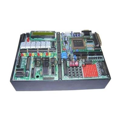
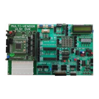
Experiments For VLSI Design Lab.
Equipment for Education, Engineering and Vocational Training
- Logic Gates - Design of Gates
- Design of AND gate
- Design of OR gate
- Design of XOR gate
- Design of XOR gate using other basic gates
- Design of 2:1 Mux using other basic gates
- Design of 2 to 4 Decoder
- Design of Half-Adder, Full Adder, Half Subtractor, Full Subtractor
- Design of 3:8 Decoder
- Design of 8:3 Priority Encoder
- Design of 4 Bit Binary to Grey code Converter
- Design of 4 Bit Binary to BCD Converter using sequential statement
- Design an 8 Bit parity generator (with for loop and Generic statements)
- Design of 2,s Complementor for 8-bit Binary number using Generate statements Sequential Design Exercises
- Design of all type of Flip-Flops using (if-then-else) Sequential Constructs
- Design of 8-Bit Shift Register with shift Right, Rshift Left, Load and Synchronous reset.
- Design of Synchronous 8-bit Johnson Counter.
- Design of Synchronous 8-Bit universal shift register (parallel-in, parallel-out) with 3
- state output (IC 74299)
- Design of 4 Bit Binary to BCD Converter using sequential statement.
- Design -
a) Mod 3 Counter -
b) Mod 5 Counter -
c) Mod 7 Counter -
d) Mod 8 Counter -
e) Mod 16 counter -
f) 4 Bit Johnson counter
- Design a decimal up/down counter that counts up from 00 to 99 or down from 99 to 00.
- Design 3-line to 8-line decoder with address latch
- Design of ALU 55 - Lab Project/Case Studies: 2 Nos.
Manufacturers and Suppliers of Experiments For VLSI Design Lab in Algeria, Argentina, Australia, Bahrain, Bangladesh, Belgium, Bhutan, Brazil, Cambodia, Cuba, Cyprus, Denmark, Ecuador, Egypt, Ethiopia, Finland, France, France, Georgia, Germany, Ghana, Hungary, Iceland, Italy, Japan, Jordan, Kenya, Kuwait, Malaysia, Philippines, Tanzania, Uganda